The glass passivated wafer/chip also included 2 types(GPP AS-CUT and GPP EPI ).The diode wafer GPP AS-CUT and GPP EPI difference as follows:
A core raw material of semiconductor products - silicon:
Formula: Si purity requirements of 99.9999% high purity polysilicon drawn from single crystal furnace.
EPI / ASCUT original wafer and diffusion theory:
(1), EPI is the abbreviation of the English Epitaxial mean epitaxy
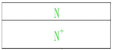
(2), silicon epitaxy process of growing a thin layer of monocrystalline silicon film is oriented on a single crystal substrate (substrate N +)
This new growth layer of the epitaxial layer (EPI layer N), the substrate and the epitaxial layer together referred to as epitaxial wafers,
English said the EPI-Wafer
(3) Structure:

Substrate resistance (Ω.cm) :0.001-0 .005
Thickness (um): 525 ± 20
(4), EPI original wafer production principle:
Arsenic high concentration (N +) of the substrate side, by the CVD method of depositing a layer of phosphorus-containing lower
EPI layer (N)
(5), the features:
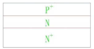
A, boron after extending structure:

B, due to substrate incorporation high concentrations of arsenic impurity, and a small range of N zone, therefore boron expansion after VR concentrated, VF is low and concentrated
C, due to the diffusion depth of the PN junction uniform, so gold spread TRR distribution more uniform
(6), ASCUT original chip:
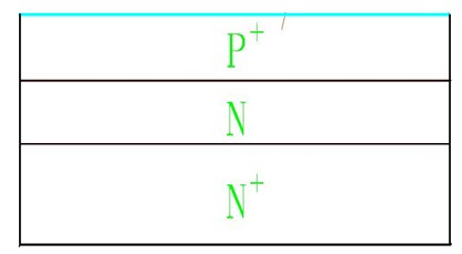
A, the original chip structure

B, the original wafer fabrication principle:
The △ taken high purity polysilicon pull into a silicon single crystal ingot according to CZ (the direct crystallization Law) or FZ (zone melting).
△ crystal pulling process according to the desired substrate concentration incorporation of impurities (P TYPE parameter into the impurity boron, N TYPE parameter into
Impurity phosphorus) into a variety of different resistance coefficient of the original crystal rod, the higher the concentration of impurities, the lower the resistance.
△ crystal rod outer diameter processed in accordance with the required chip thickness cut into a piece of the original chip, surface polishing
(Mechanical or chemical) and cleaning, to complete the original wafer process
C, diffusion principle:
△ both sides attach to the substrate (wafer) B2O3 and P2O5 and spread
△ spread structure:
 (7)EPI original chip with ASCUT of the advantages and disadvantages of the original chip:
1, theelectricalresistancebetween thecontrast:
|
Specification
|
EPI Original chip
|
ASCUT Original chip
|
|
VR distribution
|
Consistency(≤800V)
|
Inconsistent(≤1600V)
|
|
VF distribution
|
Lower and Consistency
|
High and Inconsistent
|
|
TRRdistribution
|
Consistency
|
Inconsistent
|
|
Dice total yield
|
High
|
Low
|
|
Reliability
|
Better
|
Poor
|
2, the the passivation structure classification of the advantages and disadvantages of contrast: |

